



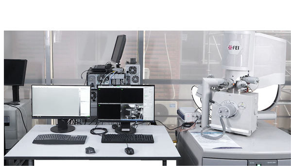
System Component | SEM and Electron beam exposure pattern generator |
Manufacturer of SEM | FEI company(USA) |
Model of SEM | Quanta 200FEG |
Specifications of SEM | 1.0 nm at 30 KV (SE) in high vacuum 3.5 nm at 3 KV (SE) in high Vacuum Accelerating voltage: 200V~30KV |
Manufacturer of Electron-beam exposure pattern generator | Raith (DE) |
Model of Electron-beam exposure pattern generator | ELPHY Quantum |
Specifications of Electron-beam exposure pattern generator | 1. Scanning frequency: 6 MHz 2. Dwell time: 167 ns 3. Whitefield alignment: Hardware correction |
Application and uses | The main application of the system is for SEM lithography, The system can be applied to the research of microelectronics, micromechanics, and micro/nano optics. |
Contact | Yujie Han |
Tel. | 65880320 |
yjhan@suda.edu.cn |
Editor: Wenchang Zhu