[an error occurred while processing this directive]

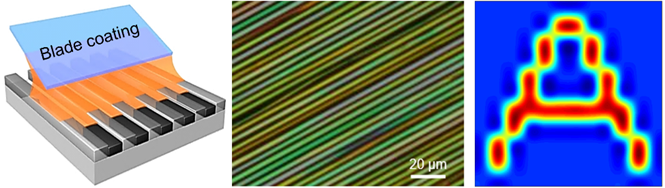
Recently, the research group of Prof. Xiaohong Zhang and Prof. Jiansheng Jie from the Institute of Functional Nano and Soft Materials of Soochow University reported a new strategy for confined crystallization of micro-channels, using the blade coating method to realize large-area, high-quality CH3NH3PbI3 with uniform morphology Perovskite single crystal arrays. The in-situ observation of the growth process and the corresponding hydrodynamic simulations prove that the microchannels introduced on the substrate surface can effectively constrain the fluid flow in the channels, and by limiting the size and shape of the contact lines, it can effectively stabilize the fluid mass transfer and reduce the contact lines. Front end nucleation density. In this case, uniform nucleation near the contact line and formation of high-quality perovskite single crystal seeds within the microchannels, followed by continuous mass transfer of the blade coating, perovskite seeds in the channel along the blade coating direction The in-channel directional epitaxial growth finally forms a highly oriented perovskite single crystal array. The perovskite single crystal obtained by this strategy exhibits excellent optoelectronic properties with high carrier lifetime (175 ns) and ultra-low density of defect states (2.0 × 109 cm-3) comparable to bulk single crystals. In addition, the CH3NH3PbI3 perovskite single crystal obtained by this method fills the entire microchannel, forming a unique embedded structure, which makes it possible to construct a perovskite single crystal-based stacked device, and each device can be realized address access, thus enabling large-scale photodetection circuits. The integrated device exhibits excellent photodetection performance, including high sensitivity, fast response speed, high detection rate, and large linear dynamic range. Further, by using the integrated detection circuit, the authors successfully demonstrated its high-resolution imaging capability for target patterns. The above results show that this strategy is simple and feasible and can be applied on a large scale, which provides a new idea for the preparation of perovskite single crystals and their integrated device applications.
请点击此处查看原文
版权所有2021苏州大学有机单晶光电材料与器件实验室
地址: 中国江苏省苏州市工业园区仁爱路199号
Copyright© hq.njust.edu.cn 2021 All rights reserved