[an error occurred while processing this directive]

Speed is the label of this era. From 2G to 3G, 3G to 4G, and then to the advent of the 5G era, each speed change has brought about the continuous progress of human civilization. In this era of rapid development of science and technology, it is also an era in which people are more closely connected with nature, and light is the hub of the connection between people and nature, and it is light that allows us to understand the wonderful things in the world. Photodetectors play an important role in converting elusive light signals into electrical ones that we can easily recognize. Two-dimensional transition metal dichalcogenides (2D TMDCs) materials with excellent optoelectronic properties are widely used in related research on photodetectors, and various photodetectors based on two-dimensional TMDCs are constantly being designed and developed. However, due to the influence of material and device structure factors such as TMDCs material defects and persistent photoconductive effect, the response speed of TMDCs-based photodetectors is limited, often limited to tens of microseconds or even a few seconds, which will be difficult to meet The development requirements of the current high transmission rate system are contrary to today's "high-speed era".
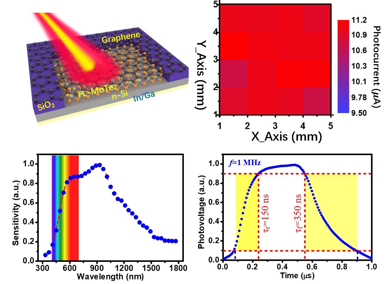
Recently, Prof Yongqiang Yu's research group from the School of Electronic Science and Applied Physics, Hefei University of Technology, and Prof. Jiansheng Jie's research group from the Institute of Functional Nano and Soft Materials, Soochow University, have conducted in-depth research on the low response speed of two-dimensional TMDCs-based photodetectors, designed and fabricated an ultra-high-speed broadband silicon-compatible multilayer (FL)-MoTe2-Si 2D-3D photodiode photodetector. The related results were published in Adv. Funct. Mater. (DOI: 10.1002/adfm.201907951). Aiming at the problems that the two-dimensional TMDCs mechanical exfoliation method is difficult to transfer in a large area, and the layered films prepared by the magnetron sputtering method have many defects and uncontrollable thickness, the researchers explored a new synthesis method for large-area preparation of 2D TMDCs-pulse Laser deposition method (PLD), realized the preparation of high-quality, large-area uniform FL-MoTe2 thin films, and constructed FL-MoTe2-Si 2D-3D heterojunction photodetectors in situ, avoiding the complexity of two-dimensional layered materials The transfer process and the interface effects introduced by the transfer process. Using a vertical n-n-type heterojunction design, the built-in electric field at the heterojunction interface accelerates the separation of photogenerated carriers. In addition, by optimizing the thickness of the multilayer high-conductivity MoTe2 film, the photo-generated carrier transit time is reduced, and the response speed of the photodetector is improved. The study found that the new FL-MoTe2-Si 2D–3D photodiode has a response speed of up to 150 ns, an electrical bandwidth of 0.12 Ghz, and a detection rate of 6.8×10¹³ Jones. These performance parameters are among the leading 2D TMDC-based photodetectors reported so far. level, even comparable to the performance of some commercial Si and Ge photodiodes. In addition, the photodetector has a broad spectral response of 300-1800 nm, which broadens the response range of Si-based photodetectors in the near-infrared band. The unique vertical n-n heterojunction design and the preparation of ultrathin layered MoTe2 films provide a new idea for the construction of high-speed and wide-spectrum silicon-compatible 2D–3D heterojunction photodetectors.
版权所有2021苏州大学有机单晶光电材料与器件实验室
地址: 中国江苏省苏州市工业园区仁爱路199号
Copyright© hq.njust.edu.cn 2021 All rights reserved